STM32 PWM Input Mode
Bare-metal C driver for STM32F411CEx for STM32 PWM Input Mode.

This is a quick tutorial on how to enable and use PWM Input mode on any STM32Fx series of microcontrollers. If you are familiar with PWM, you know it can be used to control servos, signal flight controllers, and a lot more. But they use PWM as an analog signal after feeding it through a low pass filter.
STM32’s Timers are capable of not just figuring out the duty cycle (or ON time in this case) but also the total period. It comes in handy when you’re developing devices that measure a digital signal’s period and on time.
My device under test is a black-pill board with a STM32F411CEUx but the procedure is the same for almost all devices in the STM32Fx line. I’ll be using the reference manual for STM32F411CEUx and the datasheet. On page 333 of the reference manual, the explanation for PWM Input Mode (IPM)is given. The beauty of STMicroelectronics devices is their detailed documentation. This section gives the steps to initialize Timer 2 to Timer 5 in IPM. I’ll use Timer 2 as my peripheral and the corresponding input pin A.15 as TIM2 channel 1.
Registers used here:
- RCC
- GPIOA [MODER, OTYPER, OSPEEDR, PUPDR, AFR]
- TIM2 [PSC, ARR, CCMR1, CCER, SMCR, CCER, CR1]
RCC is the clock control register used to enable the clock to all the peripherals we want to use. GPIOA is used to configure the input pin. All pins of the microcontroller are set as input pins by default. So there’s no need for them to be set in this application. TIM2 is the timer I have used to demonstrate but using these steps you can use any timer of the MCU.
A test PWM signal is generated by using TIM1. The test pin is connected to TIM2.CH1 (Timer 2 channel 1) using a jumper wire. The code for PWM is given here. The initialization of IPM is given on page 333 of the reference manual. The input signal will be sampled at a frequency determined by the peripheral clock and the timer prescaler. The peripheral clock for TIM2 is 96 MHz and t = 10.42 ns. I have used prescaler as 1 (default value). It should be noted that any value written to TIMx->PSC register has 1 added to it.

Figure 1 is the block diagram of the general-purpose timer. Just by looking at the diagram, one can deduce how the input capture would work. I’m using channel 1 (TIMx_CH1) as my input. The signal on this pin will travel to the input filter & edge detector block. A valid trigger for the application is selected by configuring TS bits of the TIMx_SMCR register. Here, I have selected TI1FP1 as my input trigger. This signal can be slowed down further using a prescaler, but I’m not doing that. If you want to do it, you can by configuring IC1PSC bits in the TIMx_CCMR1 register. Remember if you use this prescaler, you have to compensate for this in the final calculation. This signal is then sent to capture compare register. This was just an overview of the operation and now here’s the code with an explanation:

TIM2 -> PSC is the timer prescaler and divides the peripheral clock. The maximum value of the is written in TIM2 -> ARR which avoids the overflow mid-capture. TIM2 -> CCMR1 stands for Capture/Compare Mode Register 1. An active input for the TIM2->CCR1 register is selected by configuring CC1S bits of the TIM2->CCMR1 register. Second active input to the TIM2->CCR1 register is selected by writing 0b10 bits to TIM2->CCMR1 register. Set CC1S bits to map IC1 on T1 (refer to Fig 1). Set the polarity of TI1FP1 to active on the rising edge by writing the CC1P bit to 0 in TIM2->CCER register. Similarly, set the polarity of TI1FP2 to active on the falling edge by writing the CC2P bit to 0 in TIM2->CCER register. Configure the timer in slave mode by setting SMS bits to 0b100 in the TIM2->SMCR register. After the slave mode is selected, the timer needs a valid trigger and that trigger is selected by writing TS bits to 0b101 in TIM2->SMCR register. Enable the captures by writing CC1E and CC2E bits to 1 in TIM2->CCER register. Finally, enable the timer by setting the CEN bit in TIM2->CR1.
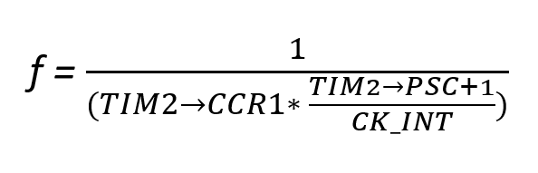
After initialization, the period and on-time can be read by reading the TIM2->CCR1 and TIM2->CCR2 registers. If you want to print frequency, use this formula:
That’s it. Thanks for your time and I hope you learned something. I’m always open to feedback so let me know what you wanna see more.
If you want to check out the code, go here 👋