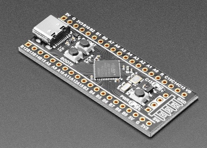
Bare-metal RCC Setup for STM32F411CEx
Run your STM32F411CEx at 96MHz without breaking a sweat.

Clock tree as shown in Fig 1 can be daunting to understand to the most experienced engineers. Going through the datasheet and reference manual gives you some idea about how the clock tree functions, but they give no clue on how to set it appropriately to run the MCU at its maximum operating frequency.

In this article, I will explain how you can set up prescalers and multipliers to achieve your desired frequency. As my desired frequency was 96 MHz, I have made the configurations accordingly, but I’ve included a formula for reference.
Every STM32F411CEx Black Pill board comes with 2 crystals. One is a 25MHz HSE (High-Speed External Oscillator) and the other is a 32.768 kHz LSE (Low-Speed External Oscillator). We’ll use the HSE as the main clock. For this, we’ll have to enable HSE in the RCC_CR register and wait till it’s ready to use.
RCC -> CR |= RCC_CR_HSEON;
while(!(RCC -> CR & RCC_CR_HSERDY)){}
If your crystal is working fine, it’ll come out of the ‘while’ loop easily and if it doesn't, you might have to rework the board with a new crystal or just get a new board. Before making some more changes in RCC registers we’ll take a small detour and set some bits in PWR & FLASH registers. In the PWR_CR register, we’ll adjust the voltage scaling options to suit our operating frequency.
RCC -> APB1ENR |= RCC_APB1ENR_PWREN;
PWR ->CR |= PWR_CR_VOS;
In the FLASH_ACR register, we’ll set the flash latency and enable the Data, Instruction, and Prefetch Cache.
FLASH -> ACR |= FLASH_ACR_ICEN | FLASH_ACR_PRFTEN | FLASH_ACR_DCEN |FLASH_ACR_LATENCY_3WS;
Back to RCC. We’ll configure the PLL before we feed the HSE clock to it. PLL_M, PLL_N, PLL_P, & PLL_Q bits of the RCC_PLLCFGR register configure the PLL. Put PLL_M = 25, PLL_P = 0, PLL_N = 192, PLL_M = 25 and PLL_Q = 4. Select PLL source as HSE oscillator by setting the RCC_PLLCFGR_PLLSRC bit.
RCC->CFGR |= (PLL_Q << 24) | (PLL_P << 16) | (PLL_N << 6) | (PLL_M << 0);
RCC -> CFGR |= RCC_CFGR_PLL_SRC;
Now configure the AHB, APB1, and APB2 prescaler. After the above configuration, the system clock is set to 96MHz. But APB1 bus has to be scaled down to 48MHz. This can be done by configuring the RCC_CFGR register. Set AHB prescaler as 0, APB1 prescaler as 2 and APB2 prescaler as 0.
RCC -> CFGR |= RCC_CFGR_HPRE_DIV1;
RCC -> CFGR |= RCC_CFGR_PPRE1_DIV2;
RCC -> CFGR |= RCC_CFGR_PPRE2_DIV1;
Turn on the PLL by setting the RCC_CR_PLLON bit in the RCC_CR register and wait till PLL is on.
RCC -> CR |= RCC_CR_PLLON;
while(!(RCC->CR & RCC_CR_PLLRDY)){}
Finally switch the system clock to PLL and wait till it is switched properly.
RCC -> CFGR |= RCC_CFGR_SW_PLL;
while((RCC -> CFGR & RCC_CFGR_SWS_PLL) != RCC_CFGR_SWS_PLL);
Call SystemCoreClockUpdate() to update SystemCoreClock variable.
And now you are done. To summarise:
RCC->PLLCFGR = 0x00000000;
RCC -> CR |= RCC_CR_HSEON;
while(!(RCC -> CR & RCC_CR_HSERDY)){}
RCC -> APB1ENR |= RCC_APB1ENR_PWREN;
PWR ->CR |= PWR_CR_VOS;
FLASH -> ACR |= FLASH_ACR_ICEN | FLASH_ACR_PRFTEN | FLASH_ACR_DCEN |FLASH_ACR_LATENCY_3WS;
RCC->CFGR |= (PLL_Q << 24) | (PLL_P << 16) | (PLL_N << 6) | (PLL_M << 0);
RCC -> CFGR |= RCC_CFGR_PLL_SRC;
RCC -> CFGR |= RCC_CFGR_HPRE_DIV1;
RCC -> CFGR |= RCC_CFGR_PPRE1_DIV2;
RCC -> CFGR |= RCC_CFGR_PPRE2_DIV1;
RCC -> CR |= RCC_CR_PLLON;
while(!(RCC->CR & RCC_CR_PLLRDY)){}
RCC -> CFGR |= RCC_CFGR_SW_PLL;
while((RCC -> CFGR & RCC_CFGR_SWS_PLL) != RCC_CFGR_SWS_PLL);
SystemCoreClockUpdate();
The formula used to set PLL frequency:
HSE / PLL_M * PLL_N = PLL_FREQFollow me on Medium at Kunal Salvi.
Instagram at Ziran_Daruwala and Blackshield Engineering.
For complete code and the latest version, check out my Github Page.
